Why do I use circuit boards?
About 90% of the DIY electronic projects I see online use breadboards. How practical are they really? Imagine if you built an IOT sprinkler control system on a breadboard and used it as a permanent solution. The idea is preposterous; one bump and a wire comes out and before you know it your grass is dead. Breadboards have their place but they aren't intended for permanent solutions. Here’s why I use circuit boards.
- Reliability: Soldered wires hold a lot better than pushed in wires.
- Neatness: It is significantly easier to troubleshoot a circuit when you can follow electrical paths rather than tracing wires.
- Size: It's easy to make devices small and compact when using a circuit board.
Why not pay for a PCB to be fabricated?
In a word; cost. Custom PCBs are extremely expensive to have produced. They also have lead times typically in the 3 week range. I can produce circuit boards with my manual process in a few hours. If I ever wanted to manufacture my devices I would definitely look at getting the PCBs professionally produced, however for most of my projects my own PCBs work quite well.
The Process
It all starts with an idea. I get my ideas from things I see in the world that could be done better. In fact in some ways I am driven by laziness. One night I was laying in bed and I realized that I forgot to turn on the heat. So I got up and fumbled in the dark for the switch on my thermostat. I thought; “with a raspberry PI and some relays I could do this on my phone in bed.” Some ideas are motivated by curiosity. “Could I really build a device like that.” Whatever the source; I come up with a concept that seems plausible.
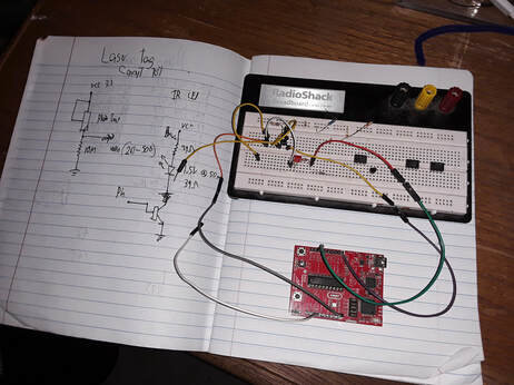
Prototyping
Often when I build a new project it uses concepts, both hardware and software, that I am not familiar with. This is where breadboards come in handy. I will prototype certain parts of the circuit to validate functionality before designing the device.
Design
My design process typically involves drawing some pictures of the device I want to make then creating a schematic. From that schematic I draw a PCB design. I usually don’t use design software for my own devices. I find that engineering paper works just fine. It’s also much cheaper than most design software applications. Since I build my printed circuit boards by hand it really would give me little advantage to design them on a computer.
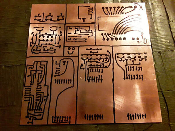
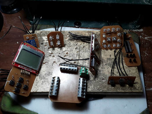
Drawing
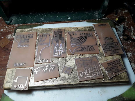
Using permanent marker I, very carefully, draw on a piece of copper-plated fiberglass PCB material. For integrated circuit footprints I will either use a stencil or I will use etch transfer paper. With one, single-sided copper board I can typically make 2-5 electronic devices so I will create a batch of projects.
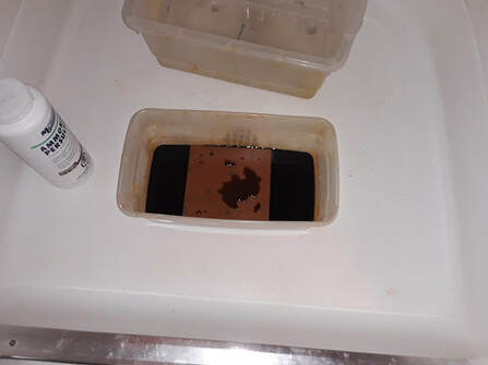
Etching
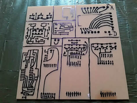
I place the copper board in ferric chloride or ammonium persulfide. The chemical etches away all the copper except that which is masked by the traces. Once completed, I clean the board with steel wool and then, in some cases, treat it with alcohol to remove all the remaining (not so permanent) ink.
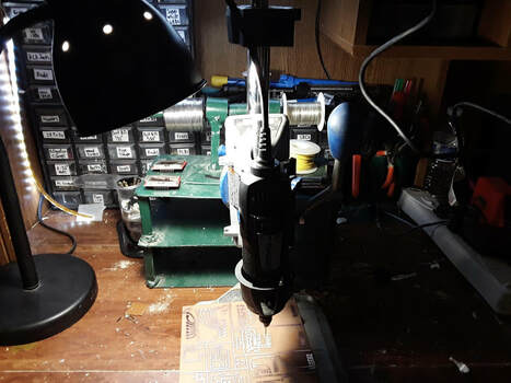
Drilling and Cutting
I use a Dremel with a 1/32” drill bit to drill out all the small component holes. Larger components require a 3/64” drill bit. In the past I would hold the Dremel like a pencil but later I got this handy stand that turns my Dremel into a tiny drill press.
Once each board is drilled, I use a hacksaw to cut apart boards for individual devices. Often I will use multiple circuit boards for one device. I then use a Dremel to cut off sharp corners and excess material as needed. Once that is complete I sand the edges for a smooth finish.
Once each board is drilled, I use a hacksaw to cut apart boards for individual devices. Often I will use multiple circuit boards for one device. I then use a Dremel to cut off sharp corners and excess material as needed. Once that is complete I sand the edges for a smooth finish.
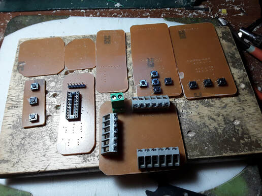
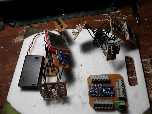
Device Assembly
I assemble the electronic devices in synchronized phases starting with the most robust component and ending with the most sensitive. This process reduces the risk that components will be damaged by soldering.
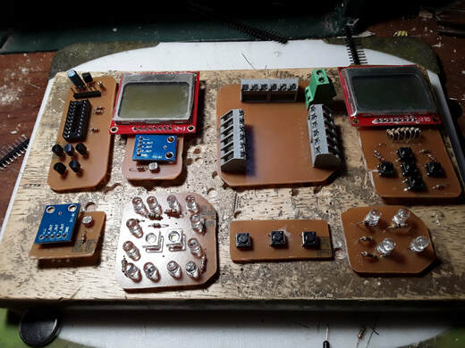
Electrical Testing
I test each electrical pathway to ensure it is conducting. I also test for shorts. Each component is tested as well; LEDs are lite up, voltages are measured across regulators, etc. At this stage I create what I call the “design guide.” This document shows me which pins go where so that later I can implement the software correctly.
Firmware Implementation
The first step to writing the firmware is what I call the “system bring up”; The interface between the microcontroller and each component is tested. In some cases minor electrical problems are discovered and corrected.
The firmware development process is different for each device. Some devices are new iterations of things I have built in the past. In that case it simply requires a few minor changes to the code. Brand new devices often require a more extensive firmware development process that can last for weeks or even months.
The firmware development process is different for each device. Some devices are new iterations of things I have built in the past. In that case it simply requires a few minor changes to the code. Brand new devices often require a more extensive firmware development process that can last for weeks or even months.
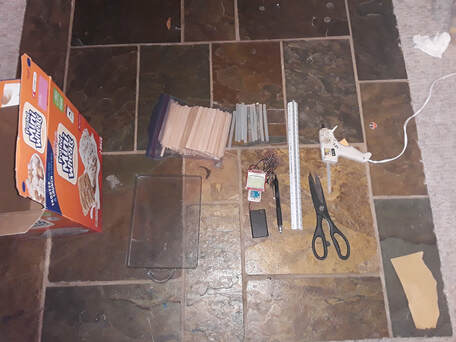
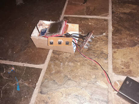
Enclosure
The final step to the process is building the enclosure. In some cases the enclosure will go on before all the programming is completed. However in most cases a device is only enclosed after it is fully programmed and the software is validated.
I have developed many types of enclosures over the years and played around with different designs, each has its trade-offs and often I will use different enclosures depending on the situation; here are a few that I have used:
I have developed many types of enclosures over the years and played around with different designs, each has its trade-offs and often I will use different enclosures depending on the situation; here are a few that I have used:
- Plastic “Radio Shack” box: Radio Shack sold these black plastic enclosures designed for housing electronics. I used these for years but ran into problems with flexibility. The black boxes came in only a few specific sizes. That made it difficult to enclose odd shaped devices like the JConsoles.
- Plexi-glass: Originally I used a “sandwich” method to enclose projects. This involved placing one piece of plexiglass under the circuit board and another on top of the device with holes for the user interface components. The advantage was it was extremely simple to make these enclosures. The disadvantage was that they offered little protection from the elements and other hazards.
- PVC Pipes: Obviously enclosing devices in PVC pipes had all kinds of issues. I would never be able to bring any PVC pipe enclosed device into an airport, for example. PVC pipe is also very heavy. Additionally installing components that needed to have wires coming out of the enclosure was difficult as the PVC pipes have very little room to work.
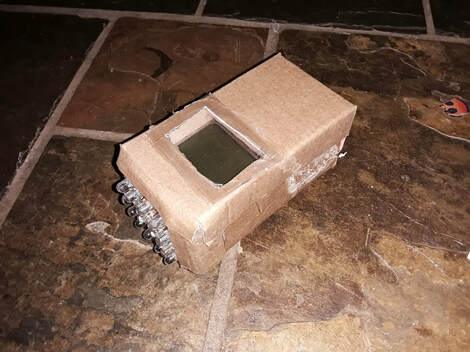
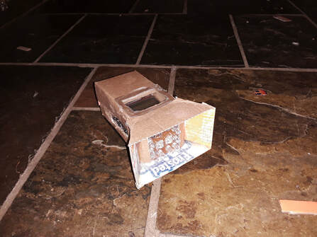
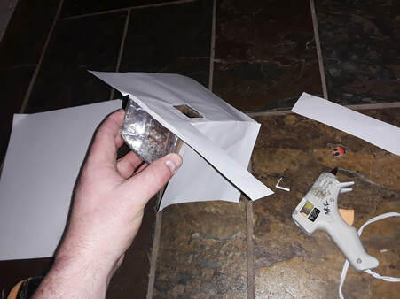
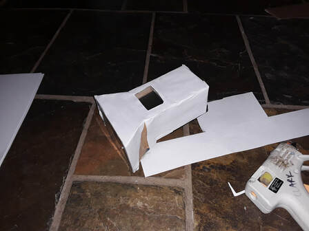
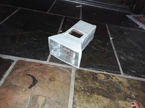
- Cardboard (the onion method): The method I have been using most recently is what I think of as “the onion method.” This involves enclosing a device in it’s own custom cardboard box. The cardboard fits tightly around the PCBs and is reinforced with wooden sticks to give it rigidity. Basically I build a wooden frame into the box and it keeps it strong. Paper is wrapped around the device for aesthetics and to seal the cardboard mechanically. In some cases use packing tape to add some water resistance to the device. I have found this method works quite well; devices can be made very small and are highly durable. Cardboard is also highly abundant and very inexpensive.
Why not 3D print a case or have one designed?
Cost and time. 3D printing also takes far longer than just building a case.
Conclusion
I have built many electronic devices using this method. Each time I do I learn something new and develop something useful.
